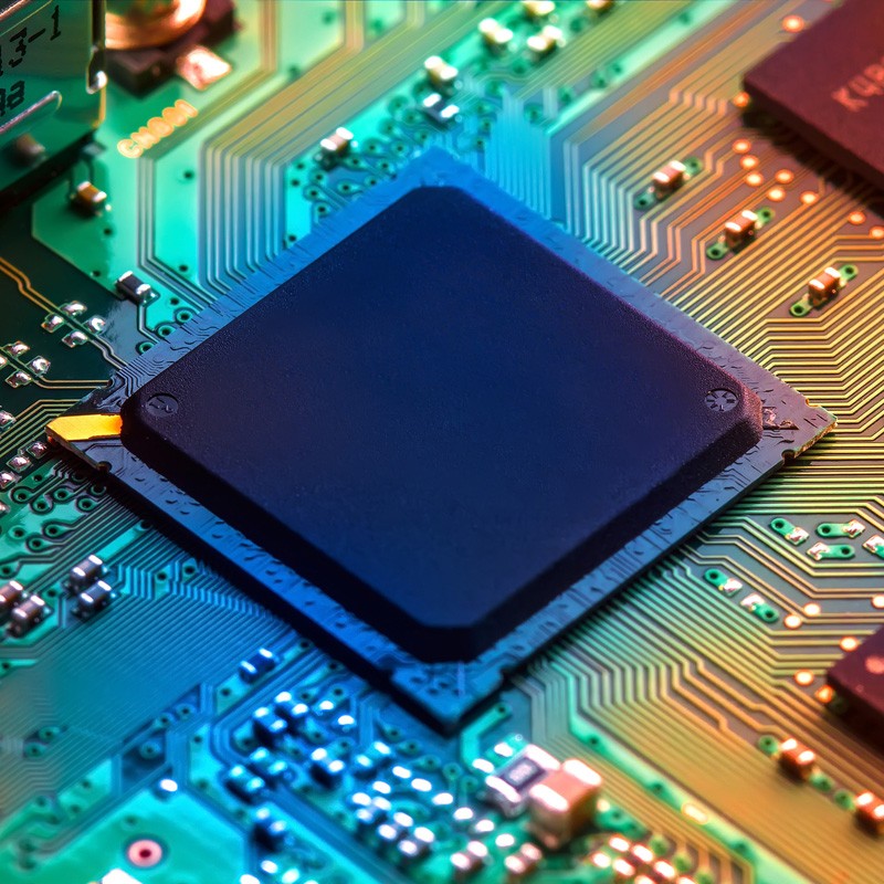
A semiconductor product includes layers of semiconductor materials arranged according to a predetermined three-dimensional pattern to perform electronic functions. A semiconductor product is manufactured by electrochemical processes which include photolithographic steps using masks to create the three-dimensional pattern.
The series of related images of the masks is a topography of a semiconductor product which can be protected to give exclusive rights to both the topography and the semiconductor product.
Ask us for advice on protecting your Topographies of Semiconductor Products.